
Why Huawei’s 2-nm Chip Patent Changes Semiconductor Constraints

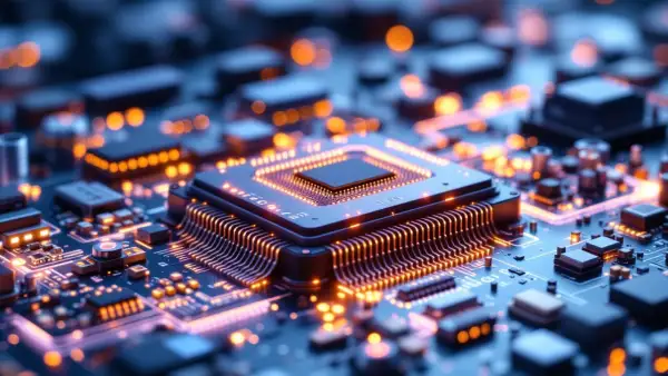
Developing semiconductors at 2-nanometre scale has long hinged on access to costly extreme ultraviolet (EUV) lithography tools. Huawei Technologies, under heavy U.S. sanctions, revived a three-year-old patent that could sidestep this critical constraint by using deep ultraviolet (DUV) technology. This breakthrough patent focuses on metal integration with pitches below 21nm, a threshold previously thought impossible without EUV.
But this move is about more than just technology innovation—it challenges the industry's assumed bottleneck of lithography capability. Huawei’s
“Constraints define competitive boundaries, not just resources.”
Why Conventional Wisdom Overestimates EUV’s Irreplaceability
Industry consensus treats EUV as an indispensable tool for 2-nm and below nodes, locking advanced chipmaking behind expensive hardware controlled by a few players. But Huawei’sour analysis of structural leverage failures.
Meanwhile, leading firms like TSMC and Samsung remain heavily dependent on EUV toolchains, locking their operational costs and scale to continuous EUV access. Huawei’s
Metal Pitch Innovation as a Constraint Bypass
The patented technique integrates narrow metal structures with pitches below 21nm using DUV. This drops reliance on EUV’s direct patterning capabilities by inserting a metal integration step, effectively achieving 2-nm-class performance. The system design works without constant human intervention, relying on a process that replicates key features without EUV’s high capital expense.
Competitors investing billions into EUV infrastructure face rising marginal costs per chip, while Huawei’sOpenAI scaled ChatGPT by optimizing model distribution instead of brute-forcing compute power, as explained in our coverage.
The Strategic Implications for Global Semiconductor Competition
The real constraint that changed is control over the semiconductor patterning mechanism. HuaweiASML—to process innovation that is replicable within its ecosystem. This undermines the assumed technological chokehold imposed by U.S. sanctions. Other countries facing similar equipment access issues, like China and parts of South Asia, could mimic this leverage move to break EUV lock-in.
This requires deep investment in metallization system R&D but avoids the near-impossible task of acquiring restricted EUV assets. Analysts monitoring global chip supply must watch Huawei’sour analysis of Nvidia’s investor shift.
“Mastering constraints, not just technology, defines future chip wars.”
Related Tools & Resources
In the rapidly evolving world of semiconductor manufacturing, companies need robust processes to stay ahead of innovative breakthroughs like Huawei's new patent. MrPeasy's cloud-based ERP solution can help manufacturers streamline production and optimize inventory management, aligning with the strategic repositioning of constraints discussed in this article. Learn more about MrPeasy →
Full Transparency: Some links in this article are affiliate partnerships. If you find value in the tools we recommend and decide to try them, we may earn a commission at no extra cost to you. We only recommend tools that align with the strategic thinking we share here. Think of it as supporting independent business analysis while discovering leverage in your own operations.
Frequently Asked Questions
What is Huawei's 2-nanometre chip patent about?
Huawei's 2-nm chip patent introduces a metal integration technique with pitches below 21nm using deep ultraviolet (DUV) technology. This approach bypasses the costly extreme ultraviolet (EUV) lithography traditionally deemed essential for semiconductor nodes at or below 2-nm.
How does Huawei’s patent challenge the semiconductor industry’s constraints?
The patent positions metallization innovation as a new bottleneck, reducing reliance on expensive EUV tools controlled by a few players. It rewrites competitive boundaries by enabling advanced chip manufacturing with DUV, signaling a strategic shift in constraint management.
Why is EUV lithography considered restrictive in semiconductor manufacturing?
EUV lithography requires highly costly, complex equipment mostly monopolized by companies like ASML. This restricts access and escalates operational costs for firms aiming to produce 2-nm class chips, locking competitors into a high capital expenditure model.
What role does metal pitch innovation play in Huawei’s breakthrough?
Huawei’s patent innovates by integrating narrow metal structures with pitches below 21nm through DUV, enabling performance on par with EUV-based 2-nm chip production. This metal pitch innovation effectively shifts the primary manufacturing constraint.
How might Huawei’s approach impact global semiconductor competition?
The new technique undermines the technological chokehold of EUV sanctions, allowing regions like China and South Asia to pursue advanced chip fabrication without EUV dependencies. This could disrupt current industry dynamics and lower barriers to entry.
What are the financial implications of Huawei’s DUV-based method versus EUV?
Competitors invest billions in EUV infrastructure resulting in high marginal costs per chip. Huawei’s method shifts fixed costs into metallization innovation steps, potentially lowering production costs and enabling scalable manufacturing without continuous EUV access.
How does Huawei’s patent relate to the concept of constraint repositioning?
Huawei’s patent exemplifies constraint repositioning by compensating for a hardware gap (lack of EUV) through system-level design innovation using DUV. It transforms the limiting factor from equipment scarcity to metallization process innovation.
Are there any existing companies heavily reliant on EUV technology?
Yes, leading semiconductor firms like TSMC and Samsung currently depend heavily on EUV toolchains for advanced nodes like 2-nm. Huawei’s patent offers an alternative that may reduce this dependency and alter industry cost structures.